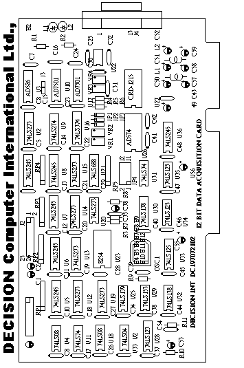
Introduction
JP1 (Jumper 1)
Determines A/D input voltage range.
JP2 (Jumper 2)
Determines unipolar or bipolar.
JP3 (Jumper 3)
Determines input mode.
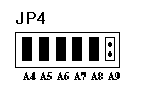
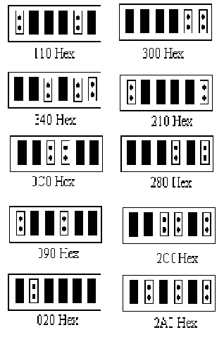
JP4 (Jumper 4)
Determines I/O port address.
JP5 (Jumper 5)
Determines AD526 (gain control factor) is used.
It is important to refer
to the user manual supplied with
your
operating system to determine the correct configuration. Please contact
your supplier if you have any difficulties with configuration.
- IMPORTANT: CARE MUST BE TAKEN IN SELECTING THE CONFIGURATION OF JUMPERS TO ENSURE YOU DO NOT DUPLICATE SETTINGS OF OTHER EQUIPMENT ALREADY INSTALLED IN YOUR COMPUTER. DUPLICATION OF SETTINGS WILL RESULT IN A MALFUNCTION OF ONE OR BOTH DEVICES.
Please refer to the
following settings for each switch and jumper
block. If you are installing more than one board, do not duplicate
jumper settings for any parameter.
JP4 is used to select
the base I/O address of the card. You may
set the base I/O address range from 000H to 3F0H in increments of F
Hex. Observe the figure below. To short a pin means that
you set it as 0, while removing the jumper means that you just set it
to 1. (A9, A8) (i.e. 0 to 3) represents the first digit of I/O
address. (A7, A6, A5, A4) represents the second digit of the I/O
address (i.e. 0 to F). The third digit of the I/O address is
always 0.
JP1 is used
to
select a
range of inputs from 0 to 10 volts or to a
maximum voltage of 20 volts. Shorting pin1 and pin2 will have a
voltage range of 10 volts, while shorting pin2 and pin3 will have a
voltage range of 20 volts.
 |
|
3.Unipolar or bipolar
Selects
unipolar/bip olar of A/D channels.
Shorting pin 1 and pin
2 selects bipolar setting, while shorting pin 2 and pin 3 selects a
unipolar setting.
 |
|
| JP1 |
JP2 |
Voltage Range |
| Short 1,2 | Short 1,2 | -5V to 5V |
| Short 1,2 | Short 2,3 | 0V to 10V |
| Short 2,3 | Short 1,2 | -10V to 10V |
| Short 2,3 | Short 2,3 | 0V to 20V |
4.Input Mode
Setting the jumper to pin 1 and pin 2 will ground the input value, so the data that will be converted should also be 0. This setting is used whenever we need to calibrate the VR or variable resistors so that the minimum voltage will be attained.
Shorting
jumper to pin 2 and
pin 3 will make use of the channel inputs to be read and converted.
 |
|
5.Programmable Gain Control Factor (AD526)
The JP5 is
used to
select programmable gain control factor, when not
short the jumper, it enable AD526, otherwise short the pin means no
AD526 work.
 |
|
For READ input
port + 0: input A/D low byte data.
port + 1: input A/D high byte data.
port + 2: read back control signal for data conversion.
port + 4: d igital I/O channel 1.
port + 5: digital I/O channel 2.
port + 6: digital I/O channel 3.
port + 7: digital I/O channel 4.
port + 8: counter 0 I/O buffer (8254 IC).
port + 9: counter 1 I/O buffer (8254 IC).
port + A: counter 2 I/O buffer (8254 IC).
port + B: counter control register (8254 IC).
For WRITE output
port + 0: select A/D channel number and enable/disable the selected channel.
port + 1: select IRQ and select control method.
port + 2: start data conversion.
port + 3: output signal to reset/retrigger IRQ.
port + 4: digital I/O channel 1.
port + 5: digital I/O channel 2.
port + 6: digital I/O channel 3.
port + 7: digital I/O channel 4.
port + 8: counter 0 I/ O buffer (8254 IC).
port + 9: counter 1 I/O buffer (8254 IC).
port + A: counter 2 I/O buffer (8254 IC).
port + B: counter control register (8254 IC).
| VR Number | Function |
| VR1 | A/D bipolar offset voltage |
| VR2 | AD574 reference voltage |
| VR3 | A/D unipolar offset voltage |
| VR4 | Offset voltage of LF398 |
VR1 is used
to
adjust the
A/D
bipolar offset voltage. JP2 should be set to pin 1 and 2 short
before measuring the voltage input. After doing so, you can check
if the values you get is half the input voltage by placing the
multimeter probe to ground and pin 12 of AD574 (U26).
VR2 is used
to
adjust the reference voltage of AD574. The probe
of the multimeter should be at the AD574 pin 10 (U26) and ground.
The value that you will read from the multimeter is 10 volts, otherwise
you should adjust the variable resistor (VR2).
VR3 is used
to
adjust the A/D unipolar offset voltage. JP2 should
be set to pin 2 and 3 short before measuring the voltage input.
After doing so, you can check if the values you get is the same as the
input voltage. You can test it by placing the multimeter probe to
ground and pin 12 of AD574 (U26).
VR4 is used
to
adjust the offset voltage of LF398, to do so, one must
short JP3 to pin 1 and 2, and make sure that JP2 is shorted at pin 2
and 3 (i.e. in the unipolar mode). After doing so, you should
place the multimeter probe or any digital voltage reading device to
ground and to LF398 pin 5 (U22) or JP1 pin 2 position. The value
that you will get should be zero voltage, if not, you can adjust the
VR4 to get the desired value.
| Pin | Function | Pin | Function |
| 1 | +12 V | 14 | 4D1 |
| 2 | GND | 15 | 4D2 |
| 3 | +12 V | 16 | 4D3 |
| 4 | GND | 17 | 4D4 |
| 5 | 3D0 | 18 | 4D5 |
| 6 | 3D1 | 19 | 4D6 |
| 7 | 3D2 | 20 | 4D7 |
| 8 | 3D3 | 21 | J3-21 |
| 9 | 3D4 | 22 | J3-22 |
| 10 | 3D5 | 23 | +5 V |
| 11 | 3D6 | 24 | GND |
| 12 | 3D7 | 25 | -12 V |
| 13 | 4D0 | 26 | GND |